Choose one
or multiple languages
0,1,1
- German
- English
- Chinese
- Spanish
IGBT

An IGBT (Insulated Gate Bipolar Transistor) is a Power semi-Conductor that can be switched off and combines the benefits of MOSFETs and transistors. In a static state, it enables powerless control, which results in minimal on-state Resistance. IGBTs are used in power electronics with switching values of up to 1,000 kVA. Key applications include switched-mode power supplies, frequency converters, direct DC converters and inverters.
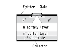
In physical terms, an IGBT has an ${n^ + }pn{p^ + }$ (or ${p^ + }np{n^ + }$) four-layer structure. The equivalent circuit can be created with a MOSFET and two transistors. Applying a positive signal at the gate forms a conductive channel between collector and emitter. Due to the p-n junction on the collector side in the conducting direction, holes are injected from here into the weakly doped epitaxy layer. This creates the electron-hole plasma responsible for the current flow. Since this plasma first needs to be built up (or reduced for switching off), the switching losses are far higher than with MOSFETs.
Latch-up is an undesirable mode of operation. When high currents are present, a transistor can latch up, as in the case of a Thyristor, due to the (necessary) feedback of the two transistors. The only way of then regaining control over the transistor is via the gate voltage when the ${V_{DS}}$ has dropped sufficiently.
